Material Characterization
- FESEM With E-Beam Lithography System
- Stylus Based Profiler
- Microscope
FESEM With E-Beam Lithography System
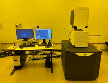
NAME OF INSTRUMENT: FESEM WITH E-BEAM LITHOGRAPHY SYSTEM
COMPANY: M/S FEI COMPANY OF USA (S.E.A.) PTE. LTD.
MODEL NUMBER: APREO 2 S HiVac
Imaging:High-resolution imagining and analysis of nano-scale research, semiconductor characterization, biological samples, and material science (morphology, film thickness,)
E-beam Lithography:Fabrication of nanometre-scale structures with high resolution and accuracy.
Specifications
| Parameter | Technical Specification |
|---|---|
| Resolution |
|
| Accelerating Voltage |
200 V – 30 kV
|
| Beam Current / Spot Size | 100 pA at 30 kV High Vacuum / Low Vacuum: 5 – 6 |
| Scan Rate |
|
Stylus Based Profiler

NAME OF INSTRUMENT: STYLUS BASED SURFACE PROFILER
COMPANY: BRUKER SINGAPORE PVT. LTD.
MODEL: DEKTAK –XT
APPLICATIONS: Surface Characterization, Film Thickness, Step heights, Trench depth, Surface roughness.
Specifications
| Specifications | Details |
|---|---|
| Measurement Type | Stylus Contact Profilometry |
| Measurement Capability | Two-dimensional surface profile measurements |
| Stylus Force | 1 to 15 mg |
| Stylus Tip Diameter | 12.5 µm |
| Sample X/Y Stage | Manual 100 mm (4 in.) X/Y, manual levelling |
| Software | Vision 64 Operation and Analysis Software |
| Scan Length Range | 55 mm (2 in.) |
| Data Points Per Scan | 120,000 maximum |
| Max. Sample Thickness | 50 mm (1.95 in.) |
| Max. Wafer Size | 200 mm (8 in.) |
| Step Height Repeatability | < 5 Å, 1 sigma on 0.1 µm step |
| Vertical Range | 1 mm (0.039 in.) |
| Vertical Resolution | 1 Å max (@ 6.55 µm range) |
Microscope
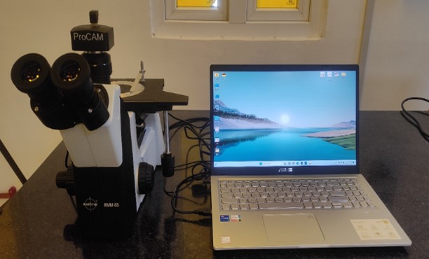
NAME OF INSTRUMENT: INVERTED METALLURGICAL MICROSCOPE WITH LAPTOP
COMPANY: RADICAL SCIENTIFIC EQUIPMENTS PVT. LTD.
Specifications