Research Highlights
Congratulations to Prof Parag Arvind Deshpande, Professor, Department of Chemical Engineering, IIT Jodhpur, for honoring with the prestigious "CSI Sistla Kameswari Young Scientist Award - 2020"

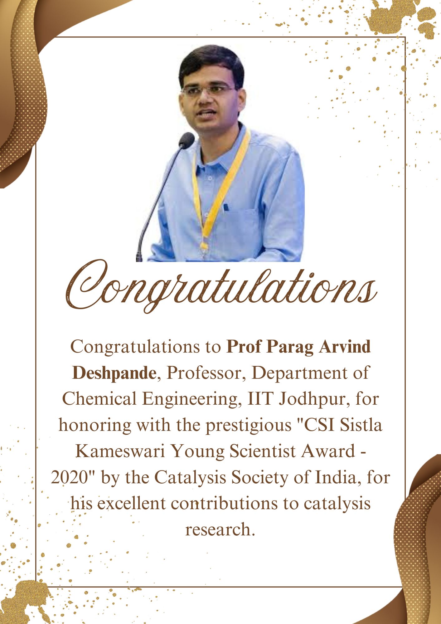
Congratulations to Prof Parag Arvind Deshpande, Professor, Department of Chemical Engineering, IIT Jodhpur, for honoring with the prestigious "CSI Sistla Kameswari Young Scientist Award - 2020" by the Catalysis Society of India, for his excellent contributions to catalysis research.
Congratulations to Prof Pradip Kumar Tewari, Professor, Department of Chemical Engineering, IIT Jodhpur, for honoring with the prestigious "Lifetime Achievement Award"

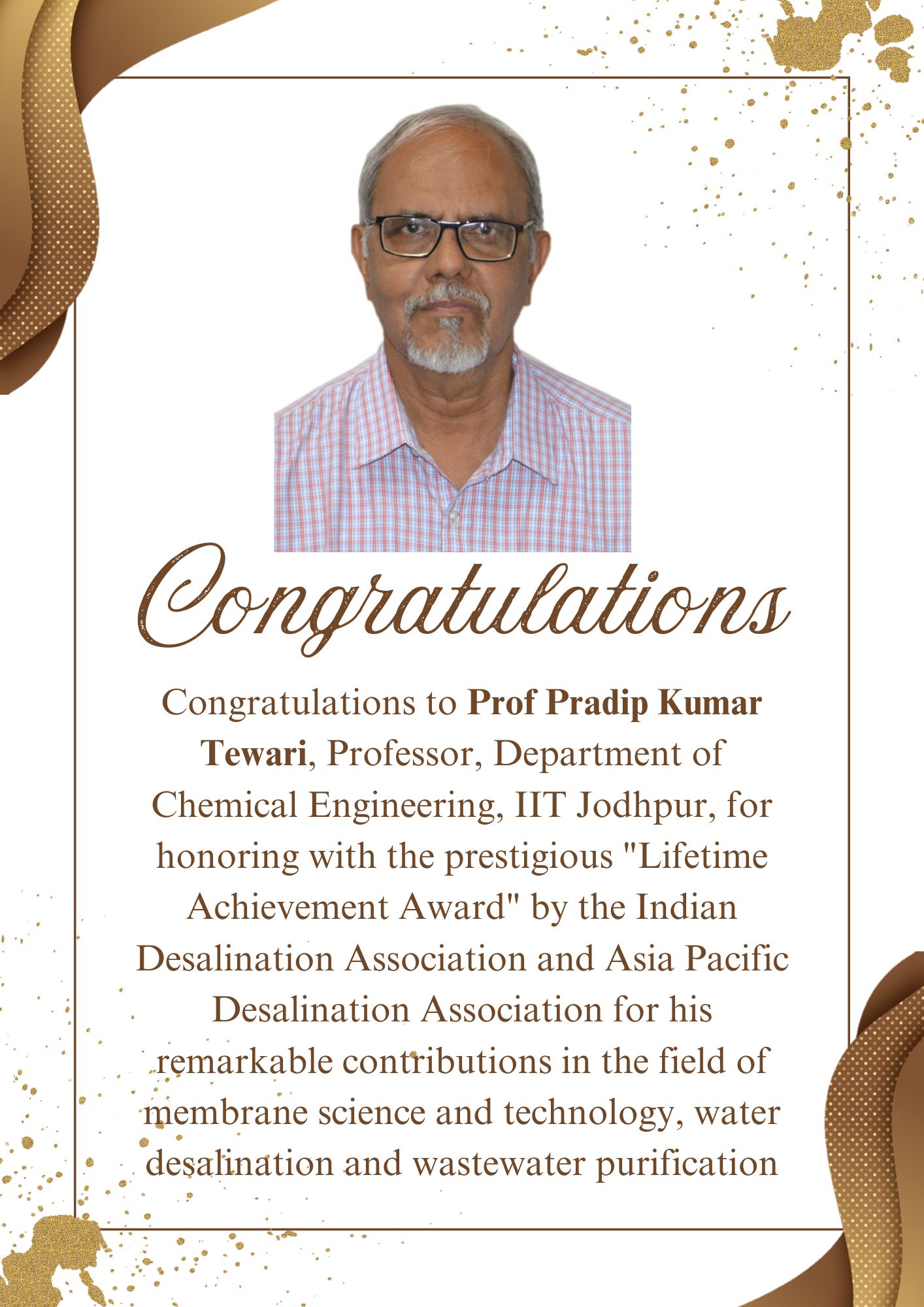
Congratulations to Prof Pradip Kumar Tewari, Professor, Department of Chemical Engineering, IIT Jodhpur, for honoring with the prestigious "Lifetime Achievement Award" by the Indian Desalination Association and Asia Pacific Desalination Association for his remarkable contributions in the field of membrane science and technology, water desalination and wastewater purification.
"Congratulations to Dr. Vikky Anand, Assistant Professor, Department of Chemical Engineering, IIT Jodhpur, for being honored as a Young Associate of INAE for the year 2025."