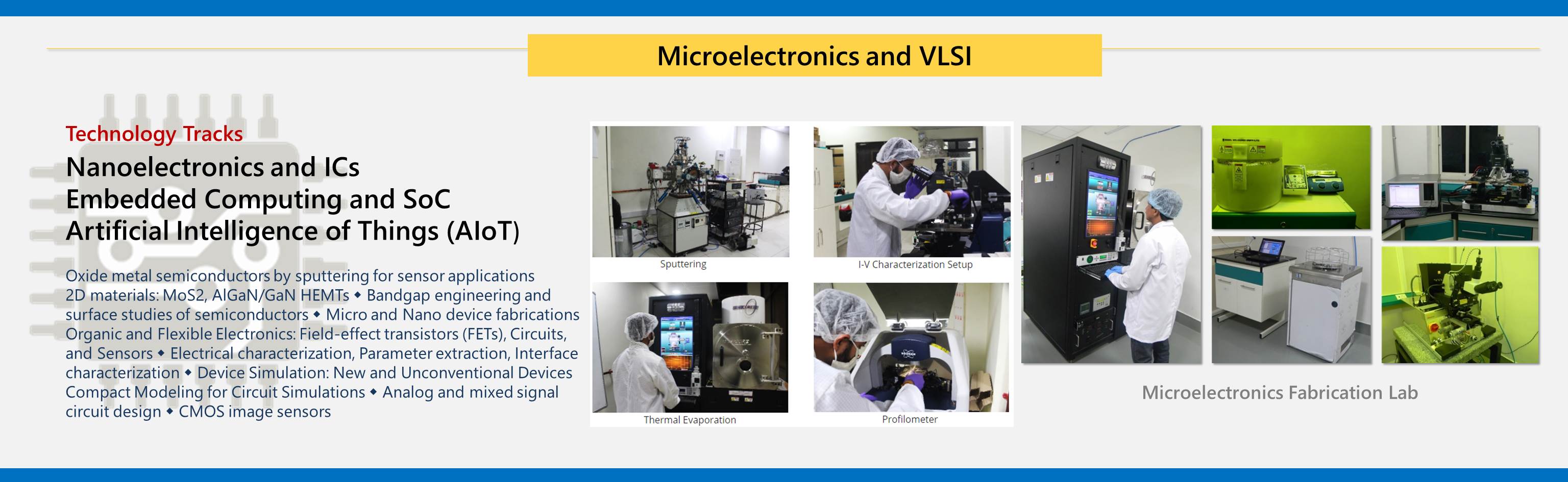
Microelectronics and VLSI
Welcome to the Microelectronics and VLSI group of the Department of Electrical Engineering at IIT Jodhpur.
Current Research Themes
- Oxide metal semiconductors by sputtering for sensor applications
- 2D materials: MoS2, AlGaN/GaN HEMTs
- Bandgap engineering and surface studies of semiconductors
- Micro and Nano device fabrications
- Organic and Flexible Electronics: Field-effect transistors (FETs), OECTs, Circuits, and Sensors.
- Bioelectronics: Electrolyte gated Transistors, OECTs, Biosensors, Wearable Devices
- Electrical characterization, Parameter extraction, Interface characterization.
- Device Simulation: New and Unconventional Devices
- Compact Modeling for Circuit Simulations
- Analog and mixed signal circuit design
- CMOS image sensors
Associated Technology Tracks
- Nanoelectronics and Integrated Circuits
- Embedded Computing and SoC
- Artificial Intelligence of Things (AIoT)
Laboratory
Facilities and equipment
- Atomic Layer Deposition for high-k gate dielectric (CNT Savannah)
- Metal Deposition System, E-beam/Thermal evaporation
- RF and DC Sputtering System
- Thermal Chemical Vapor Deposition System
- Electromagnet (up to 2Tesla)
- Keithley 2636B SMU
- Monochromator (Holmarc Spectra M01S)
- Spin Coater for solution deposition of films
- Optical Lithography : Suss MicroTec Mask Aligner (MJB4)
- Cascade 5 inch Prober, Keithley 4200-SCS Parametric Analyzer, for electrical characterization (IV/CV)
- Dektak Profiler for thickness measurements (Bruker Dektak XT)
- Gas sensing setups
- TCAD Device/Process Simulation Tools for exploration of new devices
- Laminar Flow Workbenches
- Analytical balance (Wenser MAB 220)