
Microelectronics Laboratory
This lab was developed to support the fabrication of discrete devices. It is mainly a research laboratory focusing on low cost devices and sensors for various applications. Currently, various devices such as Organic Field-Effect Transistors and Gas Sensors are routinely fabricated and characterized. Following is the summary of facilities of this laboratory

Research Themes
1. Organic and Flexible Electronics: OFETs, Circuits, and Sensors: To reduce the detrimental impact of E-waste on the earth, electronic products need to be developed which leave minimum footprints on earth at the end of their lifespan. This technology offers advantages over inorganic electronics with the possibility of development of systems on unconventional substrates that can even be of biodegradable nature. Details of this work can be found on the page of FLAME Research Group
2. Thin-Film Device and Sensor Development: Sensors based on various materials including oxide metal semiconductors, and 2D materials such as MoS2 are being fabricated for various applications using gases and pollutants. Eventual aim is to develop integrated sensors which can be enabled for IoT applications. Other Sensors such as biosensors, and MEMS based sensors are also being explored.
3. New Material and Devices: Bandgap engineering and surface studies of semiconductors, AlGaN/GaN HEMTs, Compact Modelling and Simulation
4. Hybrid Electronic Sensor Technology: HESTECH Research Group develops hybrid semiconductor devices and sensors that synergistically integrate organic/inorganic semiconductors with advanced functionalities, driving the next generation of sensor, bioelectronics, and wearable technologies. Organic Electrochemical Transistors (OECTs) use ion-electron coupling in electrolytes for highly sensitive biosensing in healthcare and environmental monitoring. OECT offers low-voltage operation, inherent signal amplification, flexibility, and biocompatibility, ideal for wearable, point-of-care, and implantable electronics. Flexible & printed electronics, made using conductive inks and nanomaterials, enable bendable, lightweight devices for various physical and chemical sensing applications.
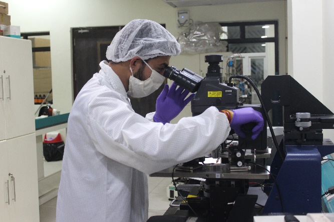
Facilities
- Device Fabrication: Mask Aligner, Thermal Evaporation System, E-beam Evaporation System, Chemical Vapor Deposition System, RF Sputtering, Atomic layer deposition, Mask Aligner, Fume hoods
- Characterization: Keithely 4200 SCS, Probe station, Gas Sensing Characterization Setup, Hall Effect Measurement, Profilometer
- Sensor and Transducer Design and Simulation Tools
(1) CoventorWare® Integrated software suite for designing and simulating MEMS sensors and actuators. A versatile FEM and BEM based tool set, has material properties database, creates or imports a 2-D layout and can build 3D models in conjunction with process flow information. Important modules consist of
- Designer - Material Properties Editor, Process Editor, Layout Editor, Foundry Design Kits
- Analyzer Meshing, MemElectro, MemMech, CoSolve, Parametric Simulations, Visualization
- Advanced Solvers and Reduced Order Modelling
(2) Mentor Graphics HEP Software: Tanner MEMS design (layout editor) and IC Design suite consist of Tanner L-Edit, S-Edit, T-spice , Eldo and Nitro SoC etc.
 |
 |
 |
 |
| Sputtering | I-V Characterization Setup | Thermal Evaporation | Profilometer |
Faculty Memebers
1. Shree Prakash Tiwari
Research Interests: Microelectronics, Organic Electronics, Microfabrication, Device Physics and Characterization
eMail: sptiwari@iitj.ac.in
Office location: Room no. 210, Department of Electrical Engineering
Phone: 0291 280 1356
2. Mahesh Kumar
Research Interests: Device Technology, Electronic Materials, Micro and Nano device fabrications, Group III-V quantum structures by MBE, Growth of thin films and nanostructures of wide bandgap semiconductors, High-k dielectrics and new chemical materials like graphene III-V Si and wide bandgap semiconductors for MEMS, MOS-HEMT Devices
eMail: mkumar@iitj.ac.in
Office location: Room no. 207, Department of Electrical Engineering
Phone: 0291 280 1357
3. Saakshi Dhanekar
Research Interests:: Nano-sensors for societal applications, bio-devices, device development, MEMS, silicon technology
eMail: saakshi@iitj.ac.in
Office location: : EE 215
Phone: 0291 280 1373
4. Harshit Agarwal
Research Interests: Industry standard compact modeling, sub-5nm devices, steep-slope transistors, emerging memory technologies, high-voltage devices, analog/RF devices and circuits, neuromorphic computing
eMail: agarwalh@iitj.ac.in
Office location: Department of Electrical Engineering, Room No. 322
Phone: 0291 280 1376
5. Ajay Agarwal
Research Interests: Microelectronics; Micro- Nano-technologies; Sensors; Micro-fluidics, Point-of-Care devices and Early diagnostics
eMail: ajayagarwal@iitj.ac.in
Office location: Department of Electrical Engineering
Phone: 0291 280 1378
6. Dr. Akshay Moudgil
Research Interests: Nano Electronics, Hybrid Transistor-based Sensor Systems, Wearable & Printed Electronics, Biosensors & Bioelectronics, Photodetectors, Molecular Electronics, Device Fabrication and Characterization
eMail: akshaymoudgil@iitj.ac.in
Office location: Department of Physics, Room No. 306
Phone: 0291 280 1383
Contact details
Room No.: The facilities are available in following room no.: 105, 219,211
Please write to one of the following for more details: sptiwari@iitj.ac.in, mkumar@iitj.ac.in